Engineered Precision: Reverse Pulse & Heavy-Duty Power Supplies
Field-proven topologies engineered for electrodeposition, micro-via filling, anodizing, and harsh industrial electrochemical operations.
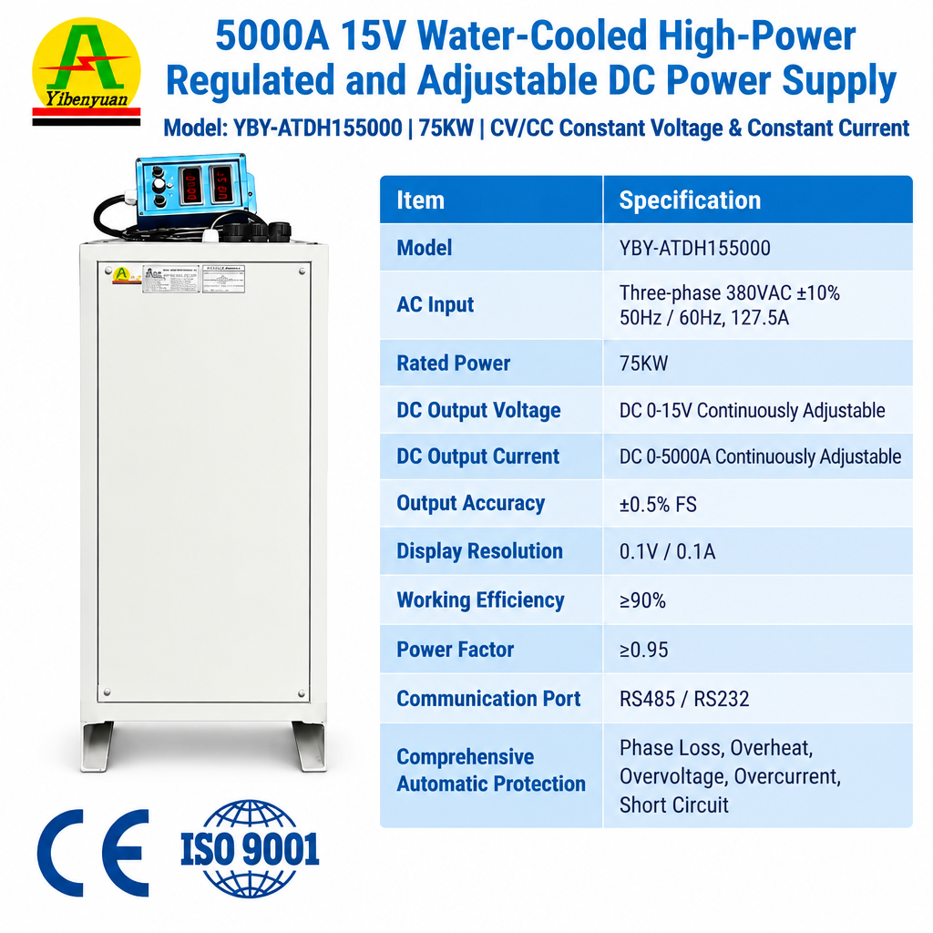
12V–15V 6000A 75kW Water-Cooled High-Frequency Rectifier
- Output: 12V/15V, 5000A/6000A
- Topology: IGBT High Frequency PWM
- Cooling: Closed-Loop Liquid Cooled
- Regulation: CC / CV Digital Logic
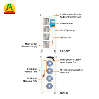
12V 4000A 48kW Heavy-Duty Plating Rectifier
- Output: 0–12V / 0–4000A Continuously Adj.
- Duty Cycle: 100% Full Load Rating
- Efficiency: ≥90% at Rated Current
- Ripple RMS: <2% Ultra-Low Fluctuation
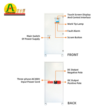
8000A 12V High-Density Liquid-Cooled Plating Unit
- Current Output: 8000 Amperes Sustained
- Protection: IP54 Sealed Electronics
- Busbar Type: Solid T2 Copper Interface
- Application: Hard Chrome & Galvanizing
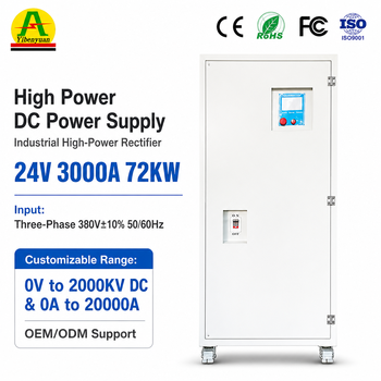
100A–3000A Precision Anodic Oxidation Rectifier
- Voltage Rating: 12V / 24V / Custom Ramps
- Program Modes: Multi-Step Current Density Ramp
- Integration: Modbus-RTU over RS485
- Use: Aviation Titanium/Aluminum Hardcoat
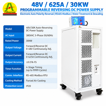
48V 625A 30kW Automatic Fast-Reversing DC Supply
- Switching Speed: Solid-State Microsecond / Relay
- Cycles: Multi-Segment Timing Profiles
- Application: Electrochemical Descaling / Water
- Control: 0–10V / PLC Isolated Logic
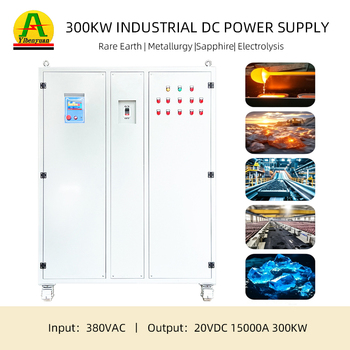
300kW 20V 15,000A High-Current Electrolysis Rectifier
- Current Scale: Up to 15,000 Amperes DC
- Power Factor: ≥0.95 with Low Harmonic Input
- Cooling Medium: Industrial Water Chiller Circuit
- Thermal Protection: Phase-Loss & Over-Temp Scram
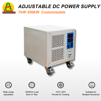
800V 50A 20kW Programmable High-Voltage DC Source
- Output Range: 0–800V DC Dynamic Sweep
- Response Time: <5ms Transient Step Recovery
- Compliance: CE, LVD, EMC Directives
- Testing Use: EV Battery, Inverter Burn-In
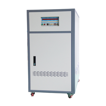
40–500kVA Solid-State Static Frequency Converter
- Input/Output: 50/60Hz to 400Hz Solid-State
- Voltage Output: 115V / 200V Pure Sine Wave
- THD Distortion: <2.5% Linear Load
- Aviation Standard: Mil-STD-704 & ISO 6858
Electrochemical Dynamics of Reverse Pulse Power Engineering
Overcoming diffusion layer limitations to achieve superior step-coverage, grain refinement, and void-free micro-via metalization.
Engineering Overview: Forward Cathodic Deposition vs. Anodic Dissolution
Standard Direct Current (DC) power supplies generate a persistent Nernst diffusion layer at the cathode interface during continuous metalization. Over extended processing cycles, metal ion depletion creates preferential current density spikes along protruding micro-profiles, leading to dendritic nodule growth, dog-boning phenomena, and unacceptable thickness non-uniformities. A reverse pulse power supply (PPR) counteracts this transport limitation by periodically alternating the polarization between a forward cathodic phase (Ton) and a brief anodic dissolution phase (Trev).
Diffusion Layer Thinning
The anodic pulse momentarily reverses the electric field, dissolving the nascent high-energy micro-asperities where ions concentrate disproportionately. This process replenishes depleted metal ions near the substrate surface, allowing operations at significantly elevated peak current densities without edge-burning.
Stress Reduction & Hydrogen Release
Electrodeposition naturally occludes molecular hydrogen within the crystal lattice, causing mechanical embrittlement and substrate delamination. Regular reverse intervals alter interfacial charge mechanics, liberating absorbed hydrogen and mitigating internal tensile stresses in electrodeposited metals.
Ultra-Fast Edge Rise Recovery
High-frequency IGBT H-bridge architecture achieves sub-microsecond current rise times (di/dt). This minimizes reactive inductive delay across busbars, ensuring square wave pulse integrity remains intact directly at the immersion cathode boundary.
| Operating Metric | Conventional Direct Current (DC) | Unipolar Pulse Power | Advanced Reverse Pulse (PPR) |
|---|---|---|---|
| Nernst Diffusion Boundary | Thick, depleted ion gradient (50–100 µm) | Partially modulated via duty cycle off-times | Actively collapsed & replenished (<5 µm boundary) |
| Through-Hole Aspect Ratio | Limited to ~5:1 without edge-burn | Capable up to ~10:1 with leveling additives | Exceeds 20:1 with uniform >90% throwing power |
| Grain Boundary Morphology | Coarse columnar structure; higher porosity | Refined nucleation, moderate density | Dense, equiaxed nano-crystalline microstructure |
| Internal Mechanical Stress | High tensile stress; hydrogen entrapment risk | Moderate stress profiles | Neutral or controlled compressive stress state |
| Chemical Additive Reliance | High dosage of brighteners and levelers | Standard bath chemistry | Reduced chemical additive footprint by up to 40% |
Future Procurement & Technology Trends: 2025–2030
Market intelligence and power electronics roadmap for next-generation electrochemistry manufacturing.
Wide-Bandgap (SiC/GaN) Power Stages
Silicon Carbide (SiC) MOSFETs are actively replacing conventional Silicon IGBTs in high-frequency reverse pulse topologies. SiC yields switching frequencies above 100kHz with near-zero reverse recovery losses, reducing output filtering volume by up to 60% and delivering conversion efficiencies above 95% across broad load profiles.
Deterministic Industrial IIoT Networks
Legacy analog 0–10V control lines are rapidly being retired in modern facilities. Procurement specifications now mandate deterministic fieldbus architectures, including Ethernet/IP, Profinet, and OPC UA over TSN. These protocols enable millisecond-synchronized recipe execution across multi-station continuous plating lines.
Closed-Loop Bath Adaptive Rectification
Procurement teams are transitioning toward self-tuning power units. Modern reverse pulse systems interface directly with real-time impedance analyzers and cyclic voltammetry sensors, automatically calculating dynamic cathodic-to-anodic ratios (If/Ir) to compensate for electrolyte drag-out and temperature drifts.
Guangdong Manufacturing Authority & Production Verification
A direct-factory manufacturing framework operating in Guangdong since 2013, validated by TÜV Rheinland on-site audit verification.
End-to-End Vertical Manufacturing Integration
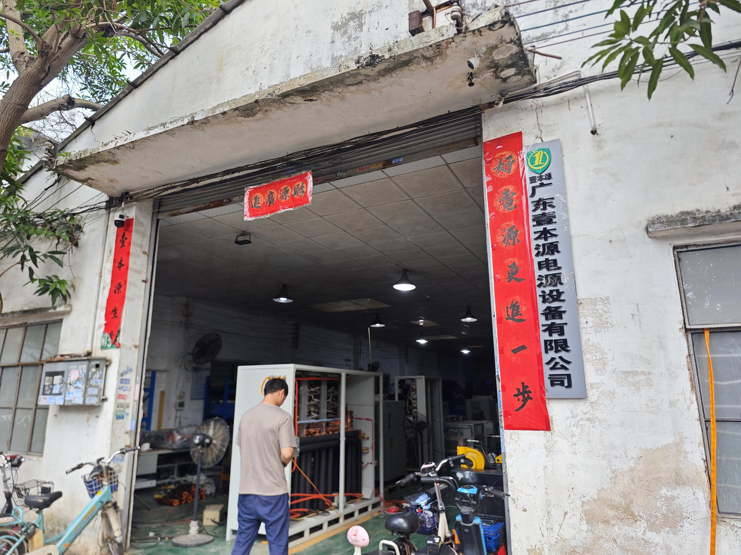
Unlike assemblers and trading entities that outsource core mechanical fabrication, Guangdong Fenvix Technology Co., Ltd. operates a vertically integrated 3,000m² manufacturing facility. Structural cabinets, low-inductance planar copper busbars, and multi-stage cooling heat-sinks are fabricated directly in-house using heavy plate shearing, high-precision punching, drilling, milling, and automated tapping equipment.
This vertical setup maintains structural and thermal control across every manufactured unit. Power electronics sub-assemblies undergo step-by-step Quality Control (QC) screening—from incoming component curve analysis to full-load inductive burn-in testing under thermal imaging monitoring.
- Direct ISO 9001:2015 Quality Management System factory certification
- CE, RoHS, LVD, and EMC conformity for global export standards
- On-site third-party audit verification executed by TÜV Rheinland
- Zero MOQ commitment: single pilot units through to fleet installations
Procurement & Technical FAQ for International Buyers
Direct answers to engineering parameters, factory protocols, and international supply chain standards.
What engineering variables must be specified for a reverse pulse rectifier design?
What factors determine whether to specify water cooling over forced-air cooling?
How are high-frequency reverse pulse waveforms preserved over long busbar runs?
What are the standard delivery lead times and batch production capacities?
Which Incoterms, payment conditions, and currencies are supported for export?
What factory acceptance testing (FAT) and warranty protections are included?
Request Custom Engineering Sizing & Factory Pricing
Connect with our power systems team to review application specs, ripple tolerances, and thermal constraints. Receive an engineering layout and commercial proposal within 24 hours.